PDP8 MOS Memory
Order Number: M8417-0-1
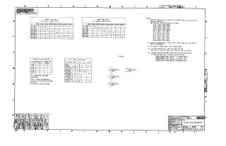
This document contains a comprehensive set of schematic diagrams for the M8417 PDP-8 MOS Memory module. It includes jumper configurations, IC pin locations, logic diagrams for memory control (RAS, CAS, and Write Enable drivers), and the memory array structure for the MOS memory components. It provides detailed engineering information for both the 16K (M8417-AA) and 32K (M8417-BA) configurations.
Site structure and layout ©2026 Majenko Technologies