PMAX System Module
Order Number: 54-19463-01
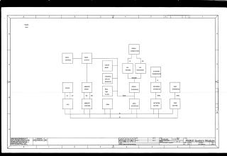
This document contains a comprehensive set of schematic diagrams and logic layouts for the PMAX System Module. It includes detailed information on the CPU/FPU/WB assembly, cache memory structures, memory controller and array configurations, ROM/memory interface, miscellaneous peripheral interfaces, serial and ethernet communication drivers, and power/reset circuitry. These technical drawings provide a low-level view of the hardware architecture, component placement, and signal routing required for the module's operation.
Site structure and layout ©2026 Majenko Technologies