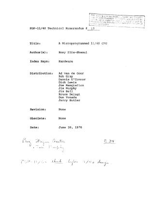
A Microprogrammed 11/40 CPU
Order Number: 13
This technical memorandum presents an analysis of a microprogrammed CPU design for the PDP-11/40. It evaluates the utilization of bipolar semiconductor components for the Read Only Memory (ROM), fast read/write scratch pad memory, and arithmetic units. The document includes a flow diagram of the proposed implementation, detailed technical comparisons of various IC components in terms of speed, cost, and power consumption, and a cost breakdown for the proposed architecture. The author concludes with an assessment of the trade-offs between a microprogrammed approach and a conventional design, considering factors such as cost, performance, and future flexibility.
Site structure and layout ©2026 Majenko Technologies