Data Break Interface
Maintenance Guide
Order Number: DEC-M2362-0-1
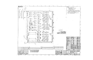
This document provides technical maintenance information and detailed logic schematic diagrams for the Data Break Interface module. It includes component lists, jumper configurations for establishing memory read/write priorities, signal definitions (such as MD_DIR, BREAK DATA G, and DATA EN H), and a breakdown of the etched circuit board layout. The document is intended for maintenance and service personnel to understand the hardware functionality and interface connectivity.
Site structure and layout ©2026 Majenko Technologies